![]()
![]()
![]()
![]()
![]()
![]()
![]()
![]()
![]()


All my content and ptohos

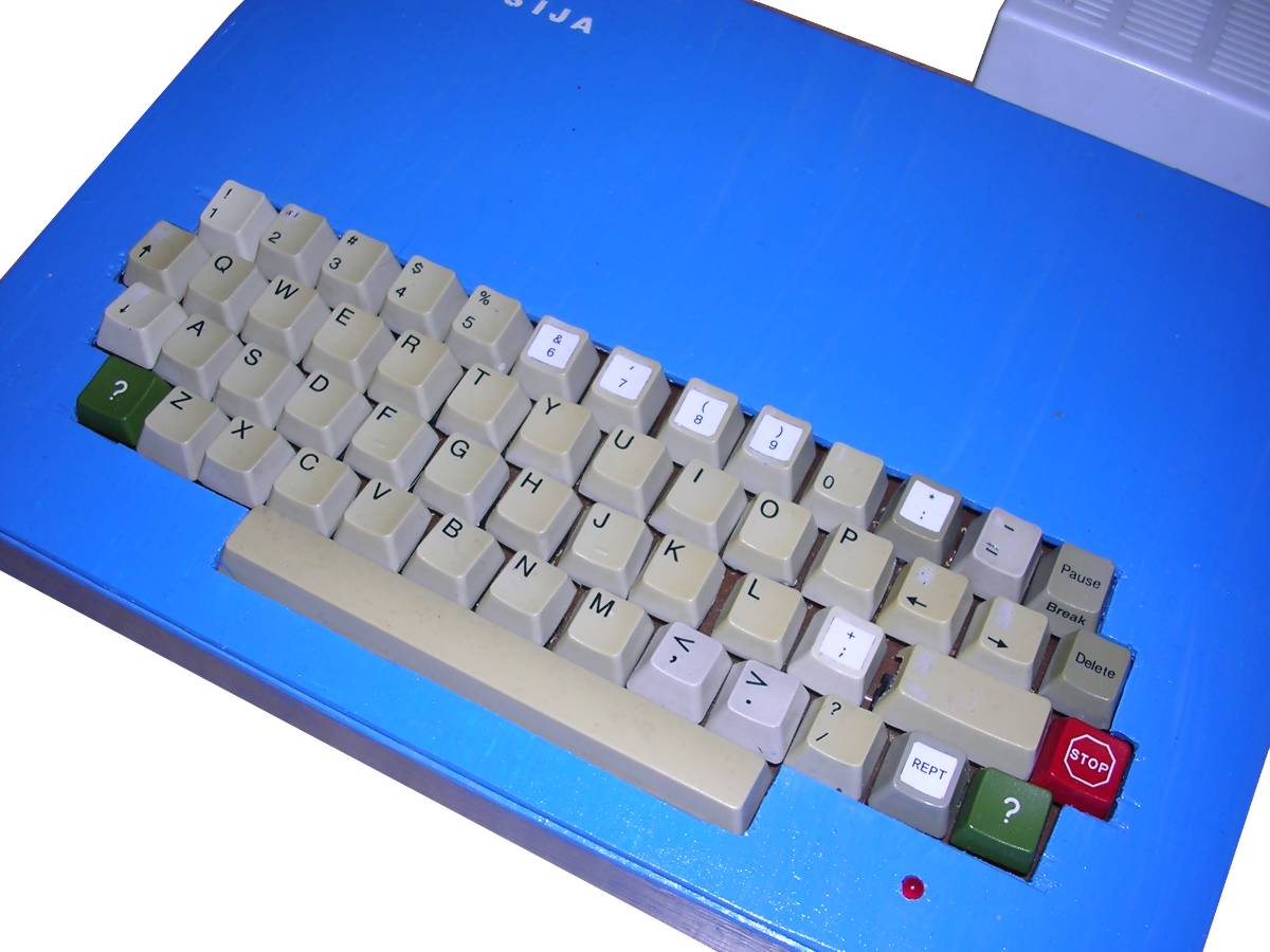
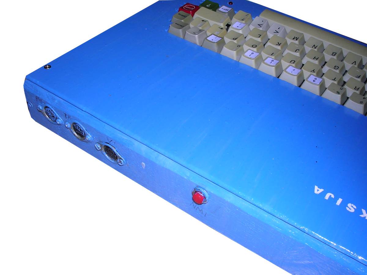
Galaksija build log
Final version
RESOURCES:
-
http://www.spetsialist-mx.ru/Galaksija/ - Galaksija site with good
schematics, PCB, ROMs
-
M.Sc. thesis about replicating Galaksija
-
http://emulator.galaksija.org/MagScans/index.html - RACUNAR Magazine scans
-
http://www.voja.rs/galaksija/galaksija.htm - More high-resolution scans.
-
http://www.dejanristanovic.com/refer/index.htm - His texts are there, use
Google if you cannot find them.
-
http://retrospec.sgn.net/users/tomcat/yu/Galaksija_list.php - Games and
programs. Most are in Galaksija's TOSEC.
-
http://emulator.galaksija.org/ - Emulator.
2018-11-09
Printing: For A4 paper and my Samsung printer,
this LO document prints out correctly, I
modified keyboard design to be compatible with my switches. It is
important to remember about ground plane which I trimmed to save
margins. They should be re-filled in PCB.
2018-11-10
I finally found cheap A4-sized sheet of copper-covered laminate.
Unfortunately it's not glass-based, but it probably will be OK.
In the top of bookcase I have an old coffee can filled with electronics
I sealed about 5-8 years ago. There are all components to build
Galaksija computer (this one with keyboard support, picture generator
and BASIC interpreter in 4kB ROM, using even BREAK string as code for
some delay routine), with sockets, passive components, even programmed
ROMs.
PCB production went bad, probably because I used a totally new and
unknown transfer media (shiny paper), I usually print on supermarket
flyers which are perfect for thermal transfer, but this time I needed
almost full A4. Removal of calcium with vinegar failed invisibly, and
the first etching left lots of copper patches unnoticed because the
laminate has the same color as darkened copper. When I saw the patches,
the toner was already washed out.
So I decided to etch one more time over entire board and look what the
result will be. The result was not good, but I think it'll work as I
removed visible copper bridges and found that track breaks can be filled
with solder. After soldering there will be more to remove.
The final fail was after I drilled a whole board with 0.5mm drill
instead of 0.8 because I got 0.5 labelled as 0.8 and had to drill again
with makeshift drill made of a broken needle.
2018-11-11
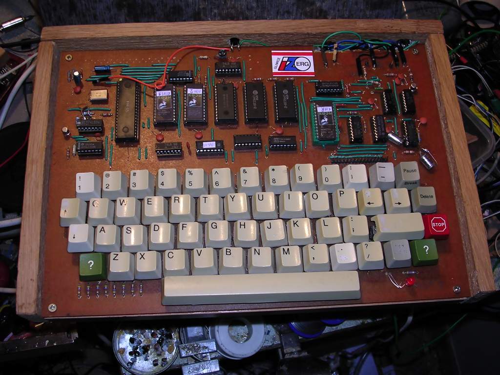
Initial assembly started. Lots and lots of jumper wires, I haven't
soldered them all. Going from right to left, jumper wires first, then IC
sockets. After I soldered copper wire as jumpers in ZX97Lite clone and
it darkened, I decided to use insulated wire with nice green insulation
where possible. So, under sockets it's impossible, and under keys too,
copper wires from network cable go there.
These nice green sockets with pin numbers won't fit as it's not too much
space between ROM/RAM sockets. I used one in character ROM.
There are more problems than I initially thought. I see that tracks are
porous, it's hard to stick solder to them and if it sticks, it sticks to
the PCB too. Soldered ROM/RAM sockets, it's hard. The only method to
finally stick the socket's pin to track was to install socket, bend pins
outwards or inwards as much as possible, brush it with flux and use
capillary forces to pull the solder: Heat the pin, push the alloy under
it.
Some tracks have visible holes, some have visible links. Before starting
it will be needed to clean the situation with an ohmmeter, soldering
iron and knife. Tomorrow: CPU region.
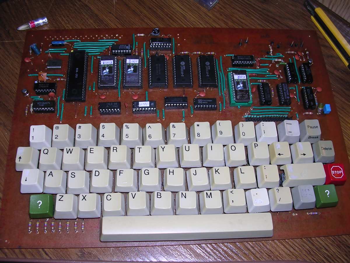
| 2018-11-18 Assembled keys, sockets, jumpers and most resistors and capacitors. There are significant problems with tracks, lots of fixing as they are "porous", so ordinary coating with alloy does not fix the problem. The keys used are a bit different than original, so I had to modify holes and it's impossible to correct their orientation as it was with original computer using a separate plate. It generally looks nicer now, no shorts on RAM/EPROMs, character ROM not tested. |
 |
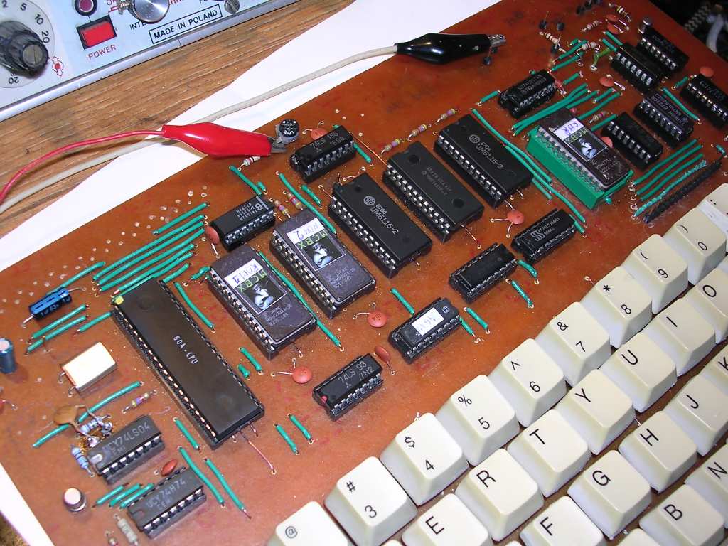
| 2018-11-20 Assembled everything. Removed more shorted/opened tracks. Startup -> No clock. Removed problem with too big cap in generator circuit, restored broken connection between inverters, clock ran, there even is something like a sync, but nothing more. Found that D0 is shorted with clock and corrected it. Still no result. No reaction to reset. There are errors in official schematic, especially related to pin numbers on glue logic. Russian schematic (Fifan's) is better, the only mistake seems to be related to data lines on 74LS174 in which two of them are flipped, but on the other side of chip they are flipped too. Additionally something seems to be wrong with resistors for video, so I'll take video from between resistors of a modulator divider. It looks like the machine bursts all components on the same logic levels, so everything goes messy. |
 |
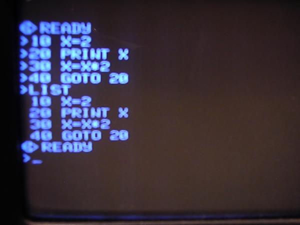
| 2018-11-22 OK, there are probably more bad connections, let's roll heavy cannons now. No boot up and CPU does some babbling on buses, activating RAMs and EPROMs. I decided to buzz through all connections using Russian schematic as a reference. Found that two chips just have no power and quite important connection to move video out is broken. Fixed and tried to boot. Partial success - there is a READY prompt, but the computer seems not to work stable way - CPU hangs, memory writes are going not where intended, and picture lines are missing, LISTing simple program returns gibberish. Because the clock is derived from a single oscillator, I decided to diagnose the following way: |
 |
| 1. Change CPU. This computer seems to work well
with a "80A MME" East German CPU... and no other. Even original
Zilog's Z80 and clone with "R" in logo break timings and it
crashes before displaying second picture line (ROMs stop to be
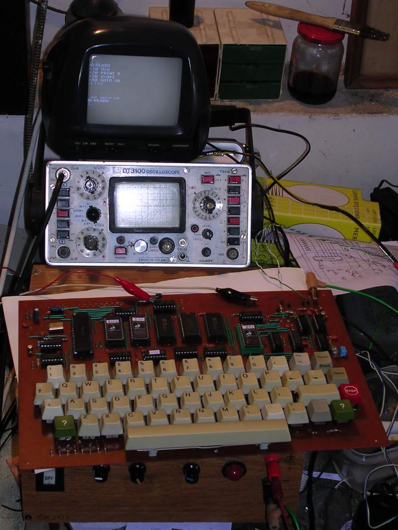
readable too early). 2. Mess with capacitors. This was a good idea. I had no other 5nF, so hacked 4n7 using soldering iron. CPU seems to run stable now, but picture is still missing random lines and... it looks like it warms up, after 20-30 seconds it's OK. 3. Mess with generator. Good that I have an oscilloscope. Now the most important thing to fix this issue: Without oscilloscope, Initiating this computer is just trial and error. Timings are critical, one gate flips too fast (still in datasheet tolerances) and data goes to the wrong place or pulse is too short. I have bought a new inverter chip for clock generator as I knew that this is a generator, parasitic capacitances in dirty connections from unsoldered 30 year old chip may kick in, gates have to be fast, don't they? Well, here NOT. The clock for pixel generation just has to be delayed specific amount of time or it will make italics. I finally found a set of logic that works with minimum capacitors added and there is this 30 year old 74LS04. Additionally, my new CD4040 (manufactured 2010) used as clock divider seems to mess timings too (firing interrupts too fast) and I had to use an old Harris chip to make it go properly. The computer successfully executed a simple arithmetic program for 15 minutes and did not hang! Draws about 0.66A of 5V, so it can be fed using 78L05 regulator. Summing up: Now I have to find a cheap casing for it. |
|
| 2018-11-24 Goes out of sync again. Replaced 74123 with LS123 although this particular 74123 has in datasheet LS's formula. Still no progress. Put 10nF instead of 5nF, a bit better. Put 6n8 in parallel - OK. When moving chips, two more problems occurred. Fixed them near 74LS32. Now video output works where it should be taken from. 2018-11-25 Generally it works. I see some small problems near EPROMs when I try to mess with them the picture gets bad, but it's not persistent and I think I'll fix it later. Made a small casing from wood, but front panel is still to be done.
|
 |
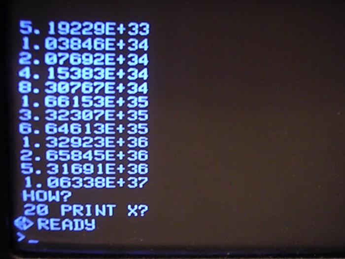
2018-11-26
If READY and prompt is shown two times, one below the other, and
pressing Return moves the next line like in a 4-5 line block, but after
few tries it moves down more, it means that negating of A7 line is
broken. If it blinks and swirls the screen with "grids" -> check EPROMs.
Now all tracks should be OK. More work on casing. Got empty on side
planks. I need about 40cm more and a front panel as the laminate sample
I got looks really poor.
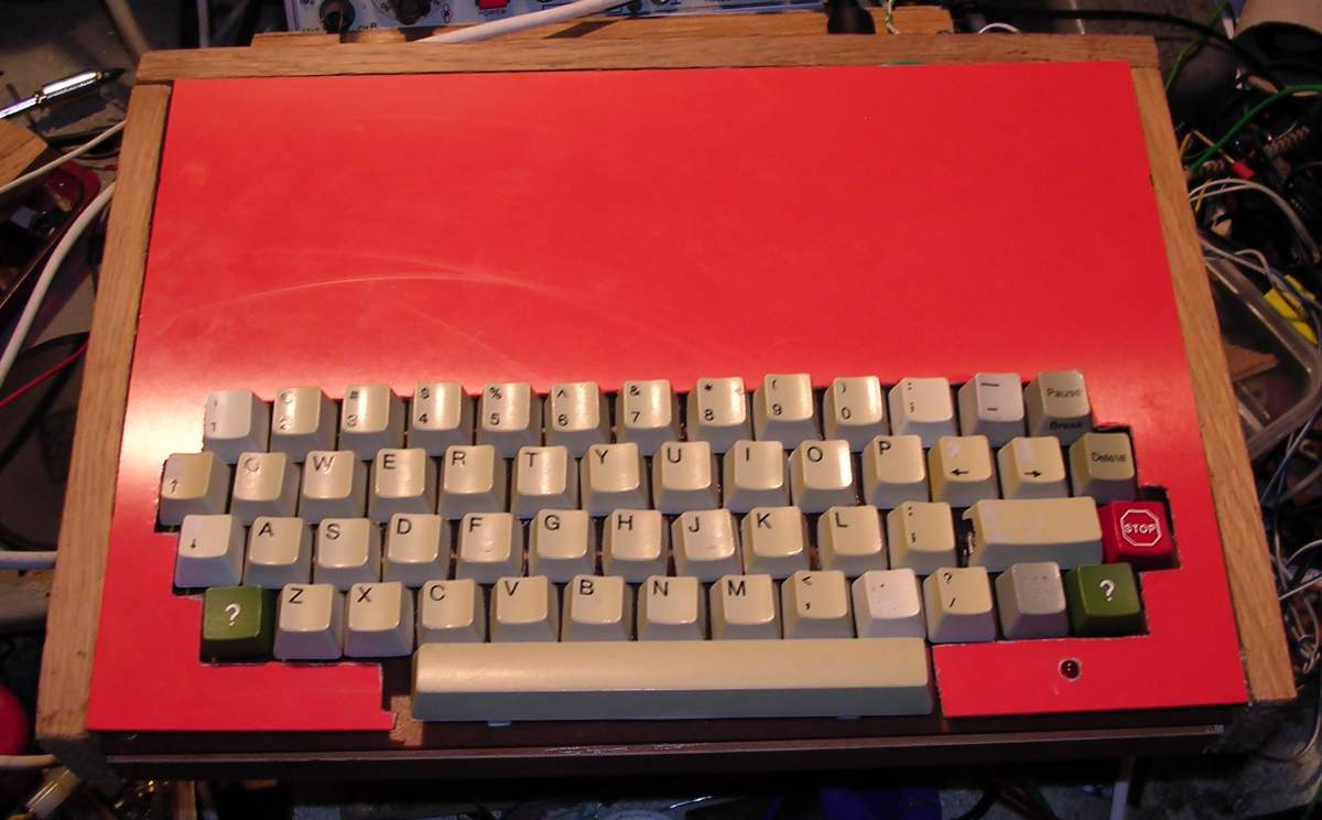
This red panel will be changed.
2018-11-27
Galaksija ROMs: There are a few variations of Galaksija ROMs. It all
comes to ROM 1, ROM A generally the main ROM, and it's related to the
second ROM. The second ROM contains a lot of useful things, additional
math functions, monitor etc. (see
Dejan's site),
but BASIC has no detection of it. To activate the ROM, it is needed to
jump to it by typing A=USR(&1000) - it will then re-set READY prompt and
functions (for writing variables) will be accessible.
To make the initial ROM jump to auxiliary ROM automatically, it is
needed to patch it writing 0xC4 at 0x03F9 and then 00 10. The next step
is bumping version number by one in 0x37 (0x1C to 0x1D, 29). As initial
procedure of bumping it was described a bit mistakenly, there are three
possible versions of ROM A:
- Without this modification
- With this modifiaction or some of its variation only
- With 29 version and modification.
ROMs available at
Spetsialist site are the second ones (only the jump instruction used
is a bit different here). I plan to use the unmodified ROM as there is
another possibility - to switch this ROM with additional 2kB of memory.
P.S. The sign that ROM2 is active should be a small shift of picture to
the right. In my unit it shifts the picture to the right by a centimeter.
Verify this!
P.P.S. All possible ROM combinations.
2018-12-12
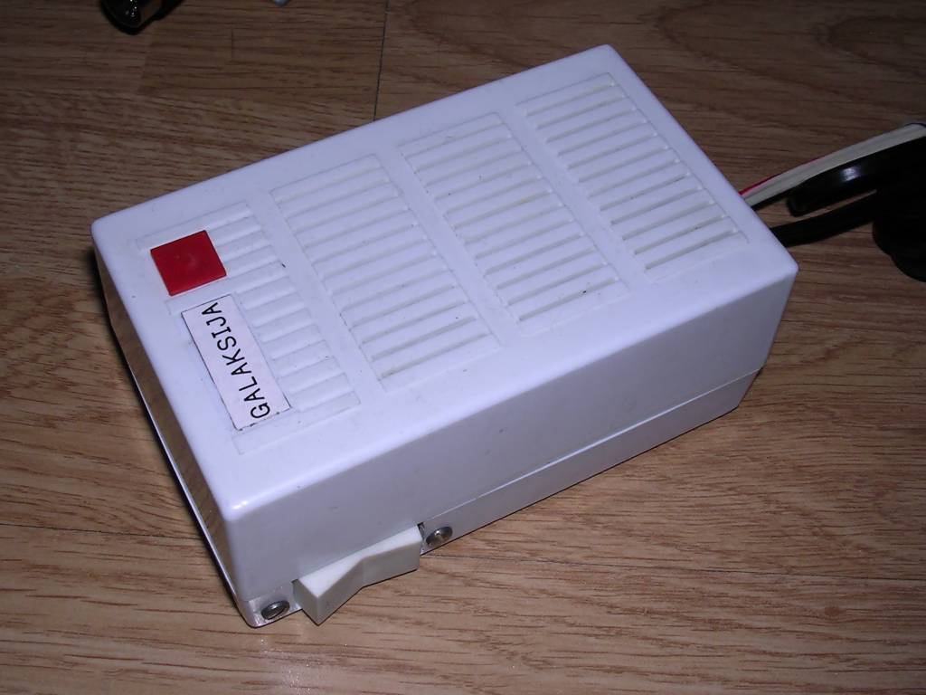
The final unit with linear PSU: